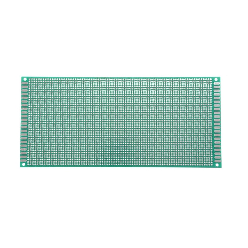
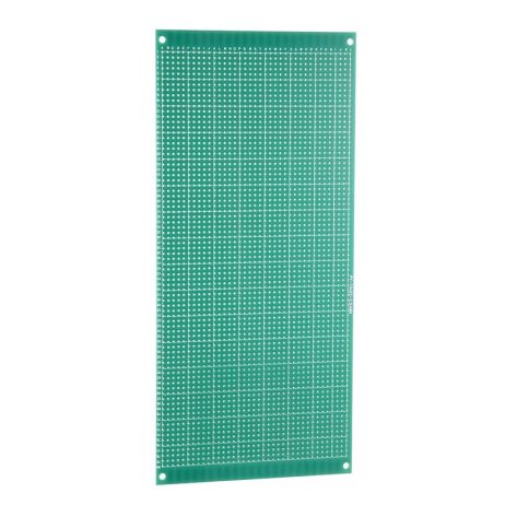

SPIDER Automation 10 × 22 cm Universal Single-Sided PCB Prototype Board
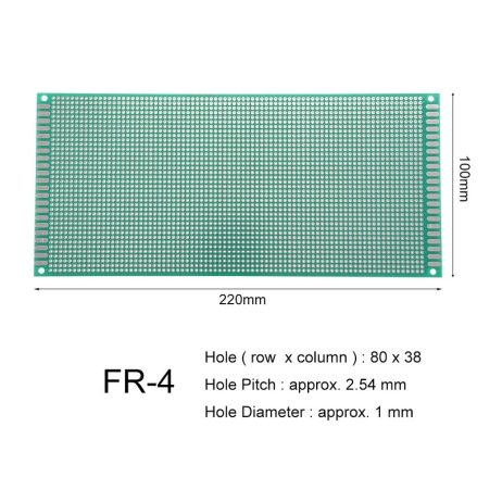
The SPIDER Automation 10 × 22 cm Universal Single-Sided PCB Prototype Board is a professional-grade circuit board designed for engineers, makers, and students transitioning their temporary breadboard layouts into permanent, robust electronic assemblies. Measuring 100 mm by 220 mm (10 × 22 cm), this single-sided perfboard provides a versatile workspace for constructing custom analog circuits, power distribution modules, and micro-controller interface boards without requiring custom PCB etching.
Constructed from premium FR4 glass-epoxy laminate with a sturdy 1.6 mm board thickness, the prototype board features precision CNC-drilled through-holes arranged in a standard 2.54 mm (0.1-inch) grid pitch. The copper traces are finished with Hot Air Solder Leveling (HASL) and coated with a protective solder resist layer, ensuring maximum oxidation resistance and clean, effortless soldering. Weighing 140 grams with a professional copper layer manufactured to international standards, this durable prototyping board delivers the mechanical stability and electrical reliability required for demanding workbench applications. Note: Product appearance and silkscreen details may slightly vary from actual images due to continuous manufacturing improvements.
Product Overview & Material Quality
Engineered to meet industrial standards, this universal prototype board combines high-grade base materials with advanced CNC machining to ensure optimal workbench performance.
- FR4 glass-epoxy laminate: Provides superior mechanical strength, flame retardation, and resistance to warping under thermal soldering stress.
- CNC-drilled holes: Automated drilling ensures precise, burr-free through-holes that accept component leads smoothly.
- HASL surface finish: Hot Air Solder Leveling coats the copper pads with a uniform solder alloy layer, preventing premature oxidation and enhancing wettability.
- Solder resist coating: Applied across the board surface to prevent accidental solder bridges between adjacent pads during component mounting.
- Toleranced copper cladding: Copper thickness adheres strictly to international manufacturing standards for consistent electrical conductivity and current capacity.
Electrical Connection & Circuit Construction
The universal grid layout supports a wide variety of wiring and component mounting techniques, bridging the gap between temporary prototyping and permanent production.
- Through-hole component compatibility: Accommodates standard DIP integrated circuits, resistors, capacitors, diodes, transistors, and pin headers.
- Point-to-point wiring: Connect pads using solid-core jumper wires, wire-wrap wire, or soldered copper bus strips on the single-sided copper layer.
- Custom cutting: Can be easily scored and snapped or sawed into smaller custom dimensions to fit specialized enclosure housings.
- Module integration: Ideal size for mounting small micro-controller boards, sensor breakouts, and supporting peripheral circuitry.
Applications
The 10 × 22 cm prototype board is suitable for a wide range of electronics development, repair, and educational activities.
- Permanent Circuit Prototyping: Soldering and finalizing working breadboard circuits into durable, permanent hardware modules.
- Educational Training & Labs: Teaching students manual soldering techniques, circuit layout planning, and hardware assembly in technical institutes.
- DIY Electronic Projects: Constructing custom audio preamplifiers, LED drivers, and sensor interface circuits.
- Embedded Systems Development: Interfacing micro-controllers with custom peripheral hardware.
- Repair & Modification: Fabricating custom replacement interface boards or auxiliary circuit modifications during equipment maintenance.
Package Includes
- 1 × Universal 10 × 22 cm PCB Prototype Board (Single-Sided, FR4, 2.54mm Hole Pitch)
Product Specifications
| Parameter | Specification |
|---|---|
| Product Category | Universal PCB Prototype Board / Perfboard |
| Board Layer Configuration | Single-Sided Copper Clad |
| Base Material | FR4 Glass-Epoxy Composite Laminate |
| Surface Finish & Treatment | Hot Air Solder Leveling (HASL) with Solder Resist Layer |
| Hole Pattern & Pitch | Standard 2.54 mm (0.1 Inch) Grid Spacing Through-Holes |
| Minimum Hole Size | 2.54 mm (CNC Drilled) |
| Copper Thickness | 1 to 4 oz (International Standard Toleranced) |
| Board Thickness | 1.6 mm |
| Physical Dimensions (Length × Width) | 100 mm × 220 mm (10 cm × 22 cm) |
| Unit Net Weight | 140 g |
| Operating Temperature Range | -40°C to +125°C Industrial Thermal Tolerance |
| Gross Shipping Weight | 0.07 kg (70 grams) |
| Shipping Package Dimensions (L × W × H) | 22.5 cm × 16 cm × 1 cm |
Connection & Operating Recommendations
- Surface Preparation: Clean the copper pads with isopropyl alcohol or a fine abrasive pad before soldering to remove any oils and ensure optimal solder wetting.
- Controlled Soldering Temperature: Maintain your soldering iron tip between 320°C and 350°C. Avoid dwelling too long on a single pad to prevent lifting copper traces from the FR4 substrate.
- Trace Routing: Plan your circuit wiring on paper or CAD software before soldering to minimize crossing wires and jumper connections on the single-sided layer.
- Thermal Management: When soldering heavy components or power wiring, use adequate thermal mass and flux to ensure solid mechanical and electrical joints.