
SPIDER Automation | 100 × 100mm FR4 Universal PCB Prototype Board | Single-Sided Through-Hole Circuit Development
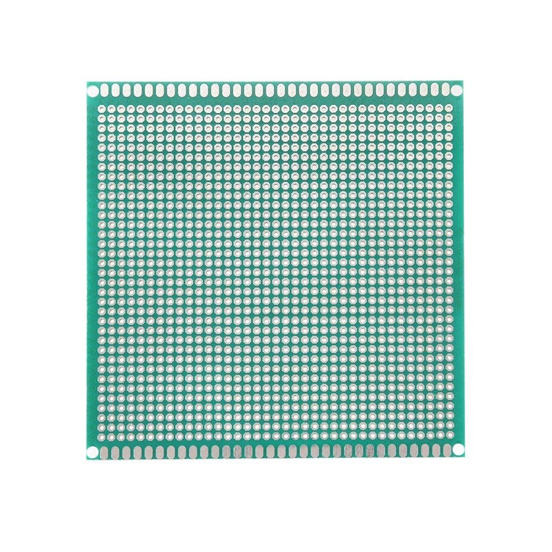
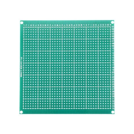
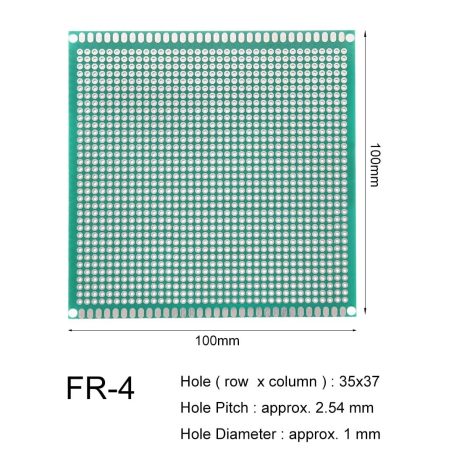
The SPIDER Automation 100 × 100mm FR4 Universal PCB Prototype Board is a general-purpose circuit assembly platform designed for developing, testing and evaluating electronic hardware using a standardized through-hole layout. Its 2.54mm (0.1-inch) hole pitch supports component placement based on a widely adopted electronics prototyping standard, helping engineers and developers arrange compatible components and connection points without designing a dedicated printed circuit board for each prototype.
Built on a 1.6mm FR4 glass-fibre epoxy substrate, this board features a single-sided copper-clad surface, CNC-drilled through-holes and a HASL (Hot Air Solder Leveling) finish. The 100 × 100mm format provides a practical working area for circuit assembly, while the copper surface allows component leads to be soldered and interconnected. For single-sided layouts requiring connections to cross, insulated wire links can be used to complete the circuit routing.
Product Overview & Construction
The board uses FR4 glass-fibre-reinforced epoxy laminate as its insulating structural material. This composite substrate provides the rigid base on which the copper circuit surface is supported. Unlike a solderless breadboard, this prototype board is intended for permanent soldered circuit assembly, making it useful when a tested circuit needs to be retained as a physical prototype.
Its single-sided copper construction provides conductive areas for soldering component leads and establishing electrical connections. The standardized 2.54mm through-hole pitch assists with positioning compatible leaded components and pin headers. Since copper is present on only one side, circuit layouts must be planned around single-layer routing, with insulated jumper wires used wherever electrical paths need to cross.
Technical Features & Functional Characteristics
- Standardized Prototyping Grid: The 2.54mm hole pitch supports conventional through-hole component placement and compatible pin-header arrangements.
- FR4 Composite Substrate: Glass-fibre epoxy laminate provides the insulating base and mechanical support for soldered electronic assemblies.
- Single-Sided Copper Layer: A conductive copper surface supports soldered component connections and circuit interconnections on one side of the board.
- HASL Surface Treatment: Hot Air Solder Leveling provides a solderable finish on the copper surface for component assembly.
- CNC-Drilled Holes: Through-holes are produced by controlled mechanical drilling to create component-placement positions.
- Square 100 × 100mm Format: Provides a defined working area for arranging circuit blocks, connectors and electronic components.
- 1.6mm Laminate Thickness: Provides a rigid substrate suitable for handling during component placement, soldering and prototype evaluation.
- Single-Layer Routing: Circuit paths can be formed on the copper side, with insulated wire links used where crossing connections are required.
PCB Layout & Circuit Assembly
This universal prototype board is intended for building circuits directly on a perforated copper-clad surface. Components with compatible lead spacing can be positioned through the drilled holes, with their leads soldered to the copper side to establish mechanical and electrical connections. The layout can be planned around the board’s 2.54mm grid to simplify component positioning and connection planning.
Because the board uses a single-sided copper layer, it does not provide independent copper routing on the component side. Where two circuit paths need to cross, insulated jumper wires should be used to maintain electrical separation. This arrangement is suitable for straightforward prototype circuits and manually assembled electronic layouts.
Applications
The 100 × 100mm FR4 universal PCB supports a range of electronics development and hardware assembly tasks where a standardized through-hole prototyping surface is useful.
- Electronic Circuit Prototyping: Building and evaluating electronic circuits before committing to a custom PCB design.
- Embedded-System Hardware: Assembling supporting circuits for microcontroller-based and embedded electronic systems.
- Sensor Interface Circuits: Developing soldered connections for sensor signal conditioning and interface circuitry.
- Control Electronics: Constructing prototype control circuits using compatible through-hole components.
- Power-Management Prototypes: Arranging circuit elements for low-voltage power-management and regulation experiments, subject to component and layout ratings.
- Signal Conditioning Circuits: Building analogue interface, filtering and signal-processing circuit sections.
- Connector and Header Integration: Mounting compatible pin headers and through-hole connectors as part of a prototype assembly.
- Electronic Module Development: Creating supporting interface and interconnection circuitry for electronic modules.
- Hardware Testing and Evaluation: Assembling circuits for functional checks, troubleshooting and design verification.
- Technical Training and Engineering Laboratories: Supporting practical circuit assembly and electronics development exercises.
Package Includes
- 1 × 100 × 100mm FR4 Universal PCB Prototype Board – Single-Sided, 2.54mm Hole Pitch
Product Specifications
| Parameter | Specification |
|---|---|
| Product Type | Universal PCB Prototype Board |
| Board Format | Single-Sided Through-Hole Prototype PCB |
| Base Material | FR4 Glass-Fibre-Reinforced Epoxy Laminate |
| Board Length | 100mm (10cm) |
| Board Width | 100mm (10cm) |
| Overall Board Size | 100 × 100mm |
| Board Thickness | 1.6mm |
| Hole Pitch | 2.54mm (0.1 inch) |
| Hole Configuration | Through-Hole Prototyping Grid |
| Drilling Process | CNC Drilled |
| Copper Configuration | Single-Sided Copper Cladding |
| Copper Thickness Specification | 1–4 oz (stated copper-weight range) |
| Surface Finish | HASL (Hot Air Solder Leveling) |
| Soldering Surface | Copper-Clad Side with HASL Finish |
| Circuit Routing Layers | One Copper Layer |
| Component Mounting Method | Through-Hole Component Soldering |
| Electrical Interconnection | Soldered Copper-Side Connections and Insulated Jumper Wires Where Required |
| Hole Spacing Standard | 0.1-Inch Standard Grid |
| Product Weight | 100g |
| Package Quantity | 1 Piece |
Installation & Operating Recommendations
- Verify Component Pitch: Confirm that component lead spacing and pin-header arrangements are compatible with the 2.54mm hole grid before assembly.
- Plan Single-Sided Routing: Design the circuit with the single copper layer in mind. Use insulated jumper wires wherever separate electrical paths need to cross.
- Check Component Placement: Review lead positions and board clearances before soldering to avoid layout conflicts and unnecessary rework.
- Use Suitable Soldering Tools: Apply controlled soldering heat and appropriate electronic-grade soldering materials to avoid damaging the substrate or copper finish.
- Inspect Solder Joints: Check for incomplete joints, solder bridges and unintended connections between adjacent copper areas before powering the circuit.
- Observe Electrical Ratings: Determine allowable current, voltage and thermal limits from the assembled circuit design, component ratings and conductor dimensions. No board-level current or voltage rating is established here.
- Clean and Inspect Before Use: Ensure the board surface and drilled holes are free from loose debris that could interfere with soldering or assembly.